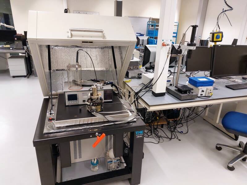
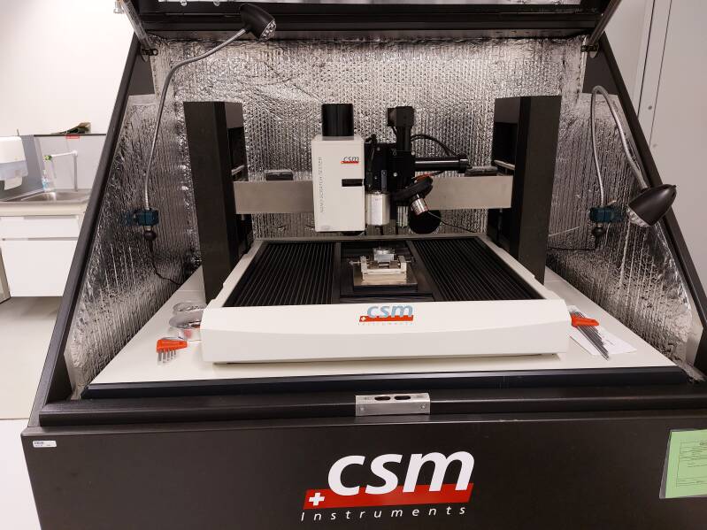
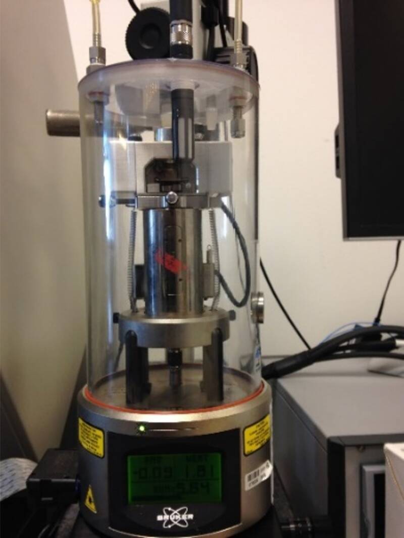
AFM's and nanoindenter of Nanoscolo
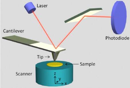
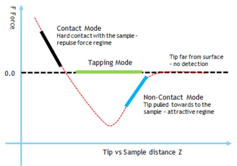
The principle is simple; feel the force during the displacement of the sample to a probe. Result is a force-distance relation of the probe approaching, optionally contacting and inserting, and subsequently retracting from the sample. Depending on the length-scale of the experiment and sample properties there are different techniques. The typical cantilever of an atomic force microscope measures forces in the order of pico Newtons to nano Newtons and the displacement by the scanner is from sub-nanometer (atomic length scale) to about 10 µm. A nano indenter is always operating in the contact mode and other force sensors may be applied in the micro Newton or milli Newton range. Still larger probes can be used pending on a balance and mechanical stages.
At the nanometers length scale the probe feels already interactions before actually being in direct contact with the sample. Vander Waals forces, electrostatic forces, osmotic forces like depletion forces, magnetic forces, steric forces and hydrophobic interaction are some examples. In contact there are also wetting forces, surface elasticity, viscous forces and elastic forces and samples can yield or fracture. Contrary to electron microscopy the samples have not to be stained or sputtered and can be measured at ambient conditions or even immersed in low viscous liquids.
For microscopy the sample is scanned to generate images. A better term than microscopy would be nanohaptics because we are not seeing (scope) but feeling (haptics) and can reach much higher resolution, nano- instead of micrometers. Therefore this technique can generate a lot of additional information compared to 'real' microscopy. Can you see whether a potato is cooked? No, but you can feel it with a fork, a typical practical indentation experiment. The fork is called a probe and many other probes can be used.
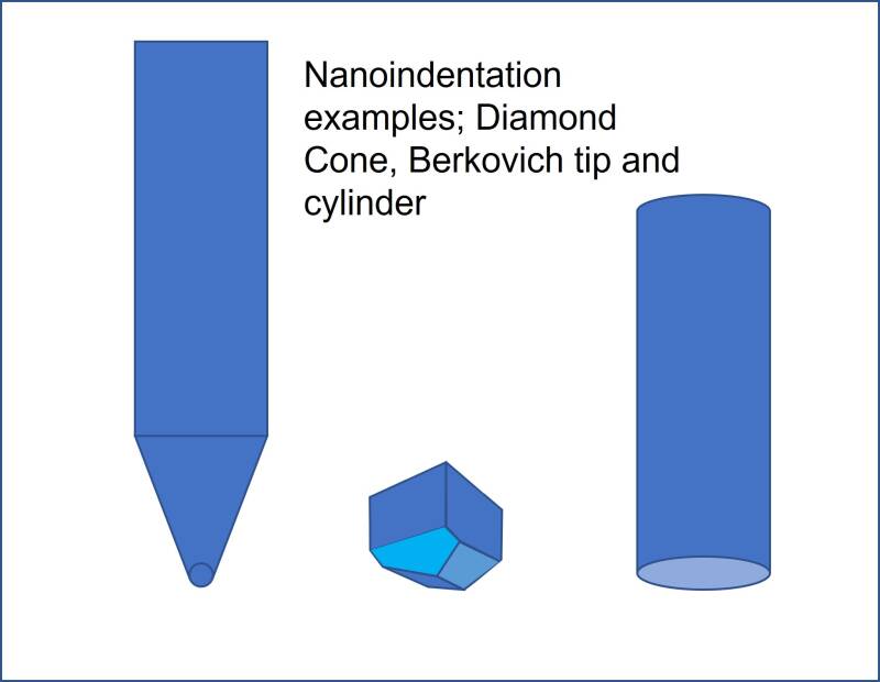
Below are some examples op probes. Easy to see that smaller and sharper probes can be used to reach a high resolution but that they easily prick and damage soft materials and are vulnerable on hard surfaces. Thin probes can bugle and for indentation probes are typically robust and made of hard materials like diamond. We also have a variety of functionalized probes. Magnetic probes, Kelvin probes and some of them will be explained in more detail.
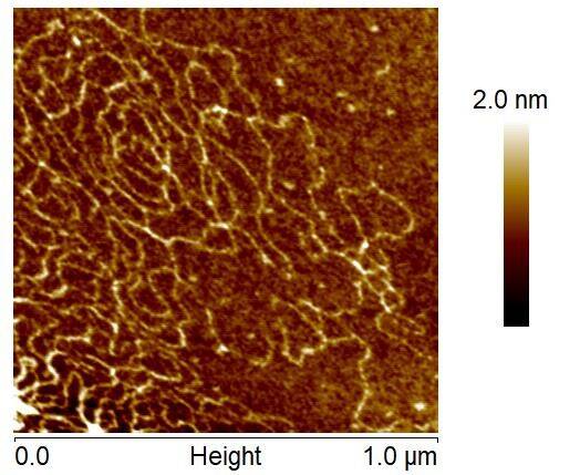
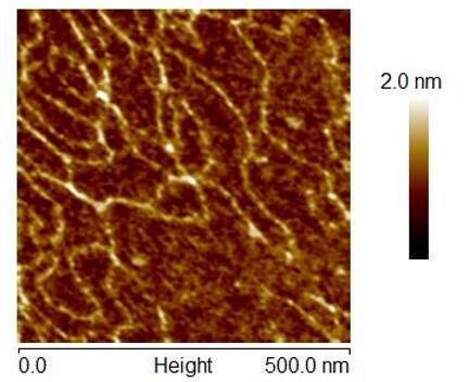
Example; DNA molecules on a mica surface
DNA molecules adsorbed on mica are laying flat on the surface and are felt at 2 nm height above the actual mica surface with a high resolution probe. The height where the probe contacts the sample is one of the parameters that can be obtained from the force-distance plots, the topography of the surface. There are numerous other possibilities, both related to surface mechanical properties and to longer range interaction forces.
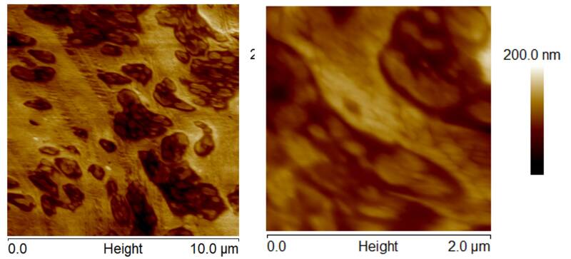
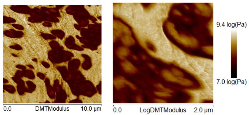
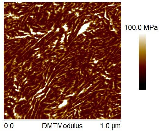
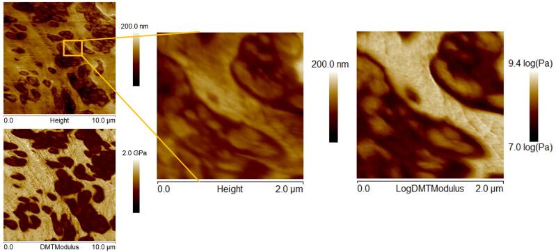
Many surfaces are adaptive to the environment, and in general the surface is different from the bulk. We can study both the surface and the bulk by making thin coupes, if necessary at cryogenic conditions. This enables to study both the bulk in fresh prepared cross sections and the surface. The atmosphere (humidity) and temperature are controlled and surface adaptation can be followed in time. For materials with multi-layers or blends and composites there is also an enormous internal interfacial area. Various aspects of this area and the different phases can be studied without staining in different environments and at nm resolution. Some examples are shown below; polymer blends and part of a Dyneema filament. Even in such a strong filament there are softer and harder domains related to the crystallites of the polyethylene.
Sometimes graphs are more clear and informative than images. They can be deduced from the images because every pixel is in fact a complete mechanical experiment. A typical example of a polar polymer that absorbs some water making it more adhesive and softer is shown above. The examples below are images that are created from the data gathered with the peak force quantitative nanomechanical microscopy (QNM) method.
Peak force quantitative nanomechanical microscopy (QNM) explained
With this technique the probe is retracted after a pre-defined load, the peak force. An example of a QNM Force-Distance plot is shown in the figures below. Every pixel of an image is obtained from such force-distance relation and several images can be obtained. For example, adhesion, modulus or deformation and the image can also be modified, revealing more details, by using linear or logarithmic scales. Below is a force-separation plot with the peakforce, adhesion, deformation and modulus indicated. Images show the effect of using linear or logarithmic data for making images of an Arnitel rubber. The peak-force that is chosen will affect the results and should be in balance with the spring constant of the cantilever, the type of probe, and the sample properties.
Other properties such as (di)electric, magnetic or piezo-electric can be studied as well and with a chemical-functional AFM tip the surface can be studied and identified chemically.
Example application on polymer blends
A "large" length scale scan area (up to 100 um) can be used to study phase separation and distribution: Both topography and modulus images show the rubber particles in dark distributed in the polymer matrix in white. High-resolution images provide detailed insight in the structure inside domains and at the interface.
The quality of polymer blends or multilayer films is related to the local mechanical properties and the morphologies of the phases and the interface. Composition and processing conditions that achieve a good product can much better and faster be identified from such images because they show quantitative effects of the multiple parameters that can be varied to make a good product. Parameters can be related to the composition, e.g. using tie-layers, compatibilizers or coupling agents and also to processing conditions, e.g. inert or in air, mixing intensity, temperature history like cooling rate. QNM can help you to optimize such parameters or give the direction how to solve problems.
Example application phase contrast magnetic, conductivity, electrostatic charge
Magnetic and electrostatic forces have a longer range than van der Waals forces and this enables to feel the topology and mechanical properties close to, and in direct contact with the surface and subsequently electric or magnetic forces after lifting the special probe (magnetic, capacitive Kelvin probe, electric / tunneling) above the surface (non-contact mode). The phase of a vibrating probe can then provide phase contrast images.
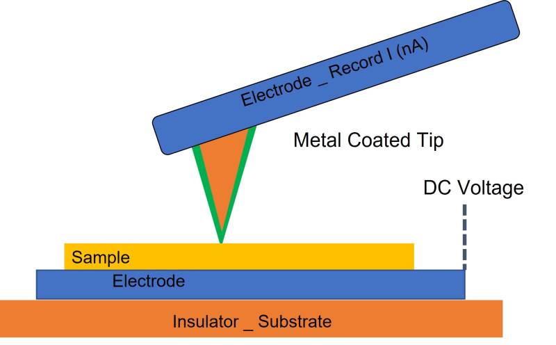
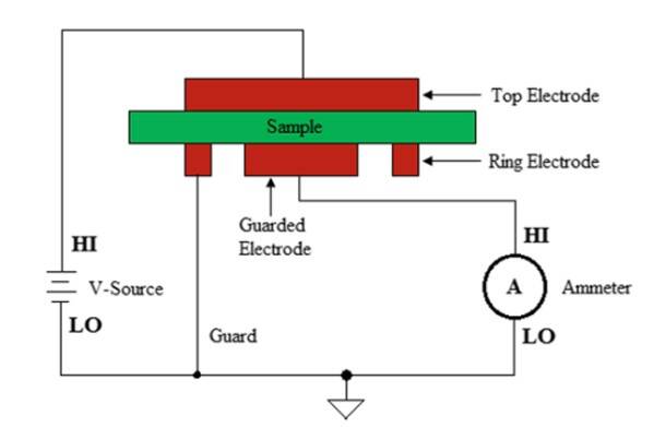
Conductive AFM (C-AFM) records simultaneously the topology and electric current (pA to nA range) via a metal coated tip. A DC voltage is applied to the sample that can be a low to semiconducting material. Below is a schematic picture of the technique as compared with a bulk conductivity measurement. The applied DC-voltage bias can be varied and the local measured volume conductivities can be integrated to obtain the bulk resistivity. In the bulk measurement the volume resistivity is AV/IT with A the surface area of the guarded electrode, V and I voltage and current and T the thickness of the sample. In C-AFM the surface area is related to the probe (and much smaller) and the calculation of the local volume resistivity is similar than in bulk but somewhat more complicated because of the different geometry.
The technique is applied in the fields of semiconductors and electronic materials but it is also useful for low conductive materials like polymers, glasses or ceramics. Below 2 examples from literature applied to thin films of nm's thickness. Like in bulk measurements the layer thickness affects the resistivity and this can be used to obtain information about the configuration of electronic materials adsorbed on an electrode. Note that the volume conductivity that is often constant for conductors or ions in an electrolyte is usually dependent on the voltage in semiconductors or if electrochemical reactions are involved.
Electrochemical AFM, EC-AFM
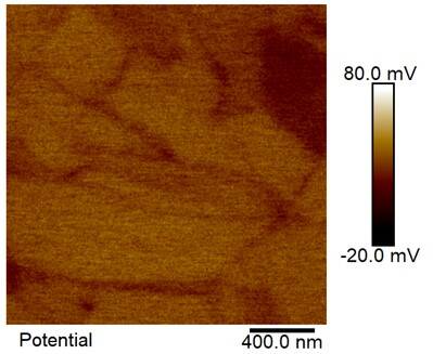
In the Kelvin probe mode (KPM) the tip is working as a capacitor at some distance from the sample. Contact potential measurements and charge density calculations can be performed. The position of the probe is kept constant by applying a voltage bias and this bias is the measured signal that equals the surface potential.
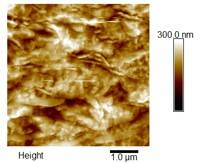
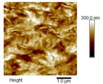
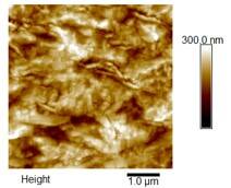
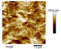
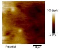
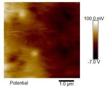
Highly oriented pyrolytic graphite (HOPG) was scanned with the environmental AFM set-up. From left to right the humidity is 2%, 30%, 50%, and 85%. A clear effect of the absorbed water on the surface contact potential can be observed whereas the morphology remains unchanged.
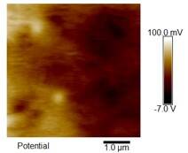
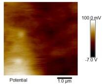
On a block-face of Teflon (PTFE), created with an ultra cryo microtome, there is a very broad distribution of contact potentials and the humidity has little or no effect. From left to right the humidity is 2%, 30%, 50%, and 85%.
In a histogram of the contact potential distributions this can be made more quantitative.
PIFM
Photo-induced force microscopy (PIFM) is an advanced technique that combines the high spatial resolution of atomic force microscopy (AFM) with the chemical specificity of infrared (IR) spectroscopy. It allows for nanoscale chemical mapping by detecting local infrared absorption at the sample surface.
The most important
Above we explained some of our capabilities related to AFM, scanning probe microscopy and nano indentation. Interesting, but not the most important. There are two more important factors that distinguish Nanoscolo from the rest;
1) The preparation of samples. SPM "feels" surfaces or interfaces (under water). Often these have to be created and we have access to the best tools to do so. An example is the UC7/FC7 Ultra Cryo Microtome of the Center for Multiscale Electron Microscopy at the TU Eindhoven that we can use with our own new diamond knives. This enables to make the perfect cut to generate the best possible cross sections with minimum cutting damage. We also have access to diverse tools of our former colleagues, e.g. the Analytical facilities of Brightlands. For hard materials like metals and ceramics we have experience with ion-beam and polishing techniques. For soft matter there are also numerous methods that we employ. Some examples include dip-coating, Layer-by-layer deposition techniques and Langmuir-Blodget coating.
2) Often underestimated is the value of decades of experience and knowledge of very many different materials and their problems. The craftmanship that is so important in this field. There are so many details that make the difference between artifacts and failure or valuable data solving your problem. We enjoy showing this to our customers, and even teaching them how it works. This mission could be your prime reason to chose for Nanoscolo.
3) At Nanoscolo, we focus on understanding the intricate details of force-depth relationships measured as a probe indents or immerses into a material. These interactions are influenced by surface tensions and energies, wetting, adhesion, nanoparticles, fouling, rheology, mechanical properties, friction, and various other macroscopic phenomena. Our expertise extends beyond Atomic Force Microscopy (AFM), encompassing a comprehensive understanding of the role of interfaces in materials and processes.